![]()
|
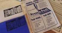
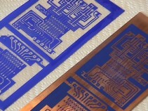
Using the press-n-peel PCB transfer film (directions).
The following is a mirror-site off the Techniks Inc. web site "How to" Please be advised the original information and the updated information can be directly obtained from Techniks web site at:
In a few short steps you can produce your own circuit boards in minutes using Press-n-Peel PCB Transfer Film. Press-n-Peel offers you the ability to take computer generated PCB layouts, and either photocopy or laser print them onto the Press-n-Peel Film, and subsequently transfer that image onto copper clad printed circuit board material.
Etch the board in ferric chloride and you have a high quality pc board in minutes. For complete directions, simply follow below 7 steps.
directions:
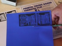
1. Photocopy
or Laser Print circuit image onto the dull side (emulsion) of Press-n-Peel
Image Transfer Film. Prepare: Clothes Iron, Steel Wool #00 and a touch of liquid soap (or SOS , Brillo), Packaging Tape, Photocopy or Laser Printed Circuit Image, & Directions.
2. Cut Press-n-Peel, leaving a 1/4" border around the circuit image. Cut board to size.
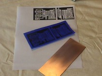
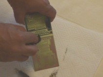
3. Clean copper board with steel wool, Scotch Brite© or Brillo© pads. Rinse cleaned board with soap and water. Be sure to remove all soap residues. Dry thoroughly with lint-free cloth. Be sure to scrape any burrs that appear on the edge of the board that may have resulted from the cutting/shearing process. Burrs tend to keep the iron from making solid contact with the Press-n-Peel Film.
4. Place Press-n-Peel with image face down onto clean copper board. Iron the Press-n-Peel Film to the board. Some users prefer placing a piece of plain paper between the iron and the film to reduce friction. Temperature setting on the iron is critical, and dependent upon your laser printer or photocopier. Suggested starting temperature is 275-325 degrees F. Iron settings generally are between the "acrylic" and "polyester" settings. Time varies with the size and thickness of the board. Generally this is 1.5 to 4 minutes. DO NOT USE STEAM!
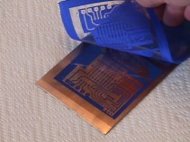
5. Quench the
board/film combination under cold running water. Peel the film off. To remove, if necessary, small "fills" in between traces and "filled donuts", cover the imaged copper board with clear packing tape, and then remove. This will pull all unwanted filled areas off the board
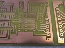
6. After removing "fills", trim the board (if necessary) to the final size. Wash the board in soap & water before etching to remove surface oxidation. Etch with any standard copper board etching solution -- Ammonium Persulfate, Ferric Chloride, etc. (Note: EID does not sell PCB etching supplies -- available through local electronic supply stores)
7.
Using steel wool, scrub the Press-n-Peel image off as to reveal copper
traces. This is best done under running water. Suggestion: Do not do this
until your ready to drill and populate the board. The Press-n-Peel
transfer resist protects the board from oxidation
|
|
|